Shenzhen Sucks...But So Do I
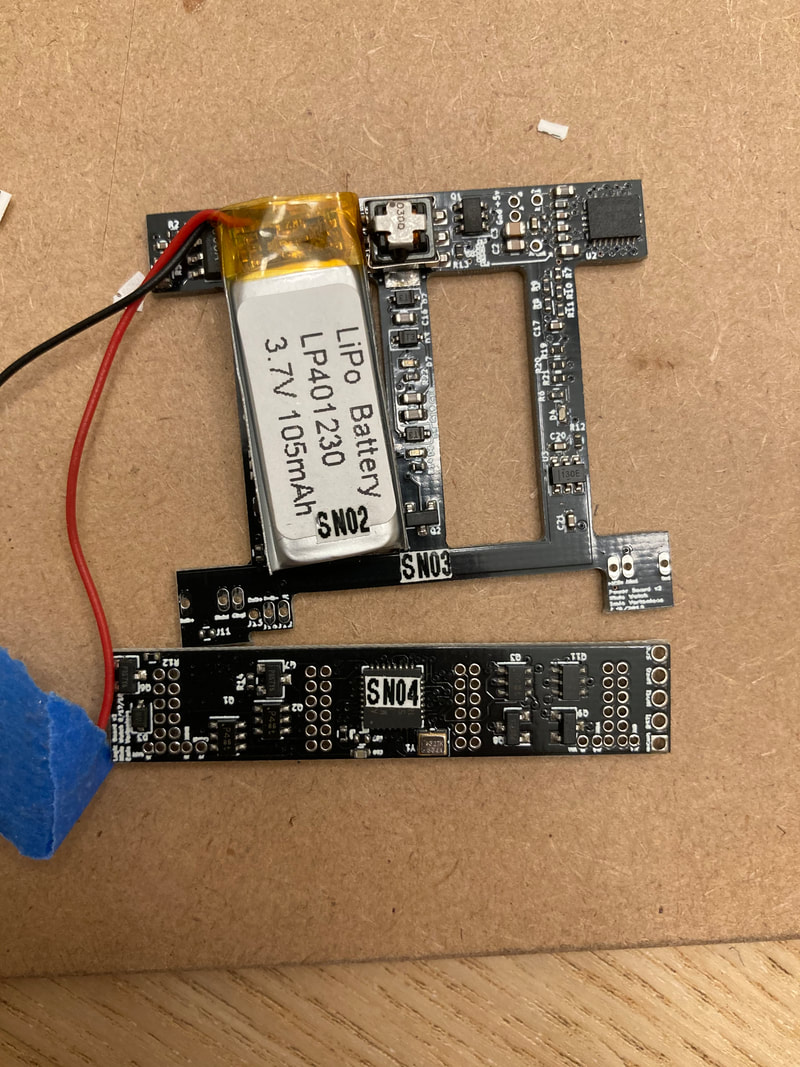
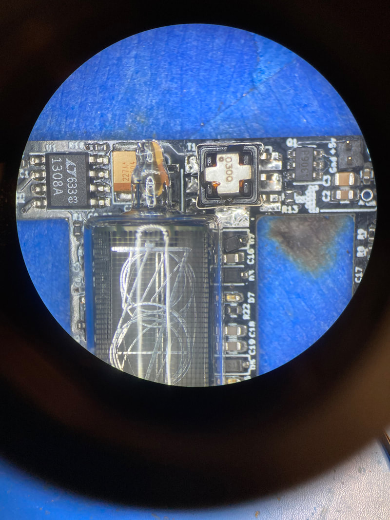
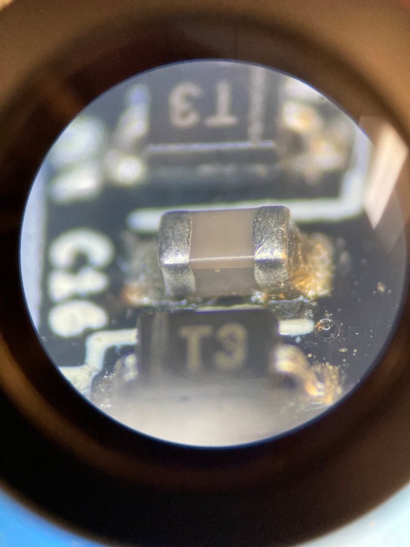
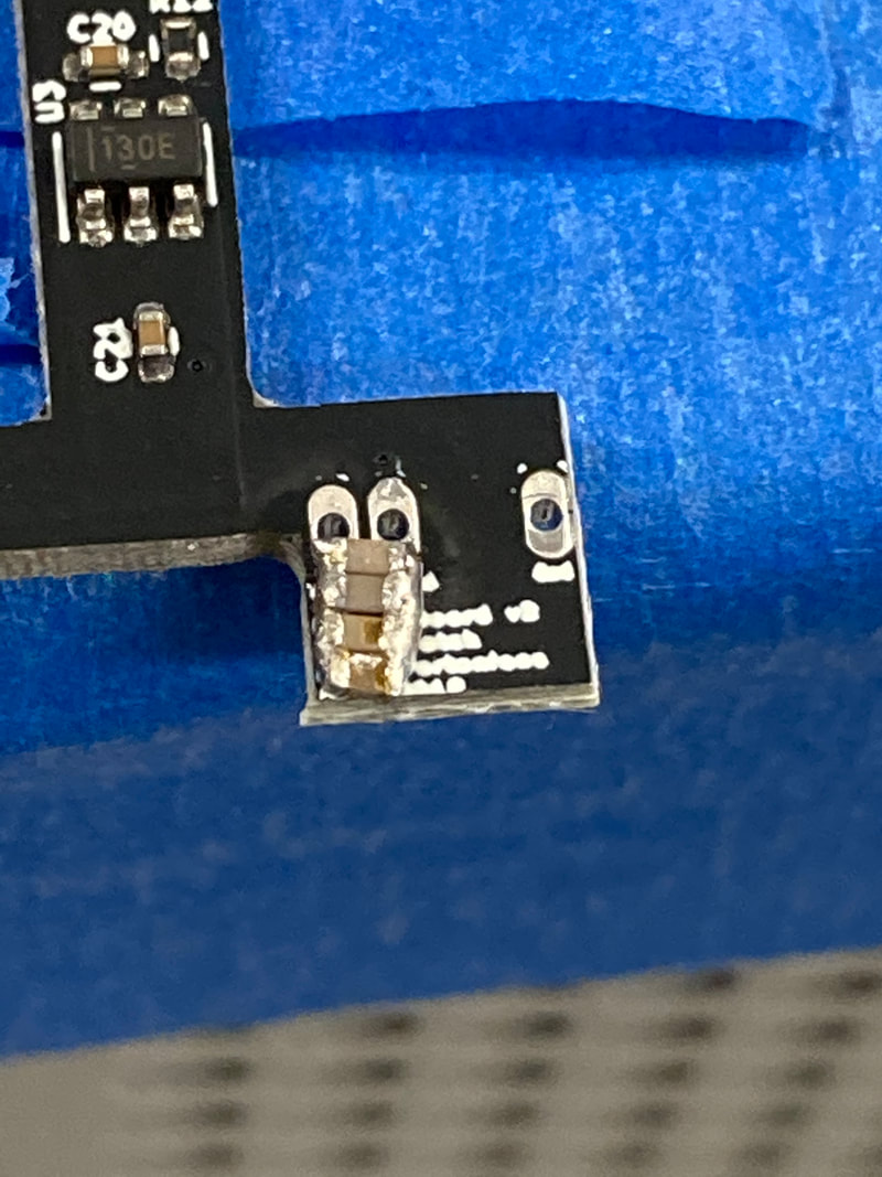
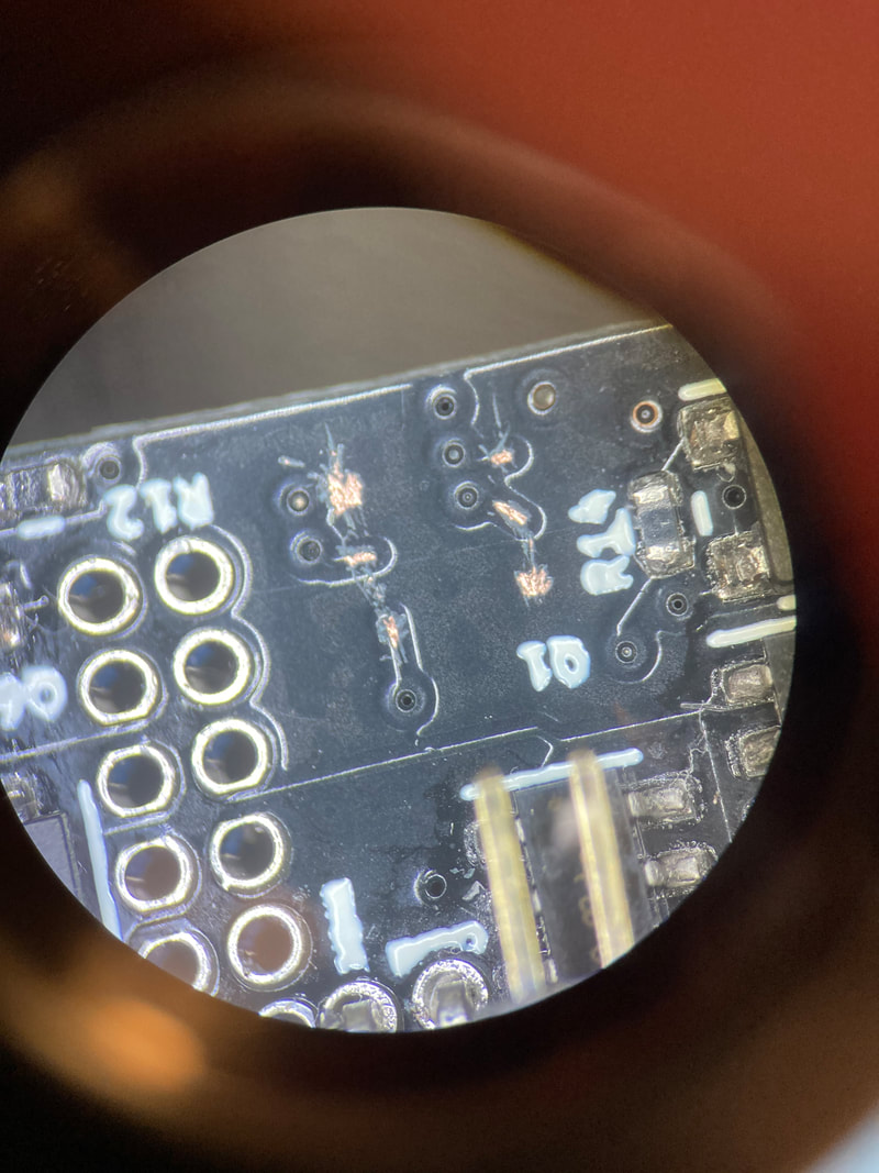
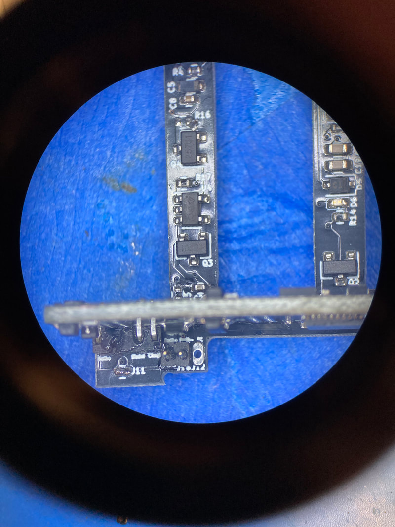
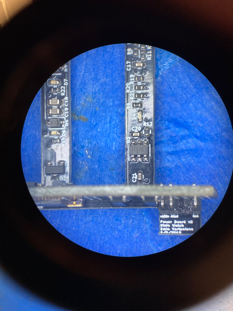
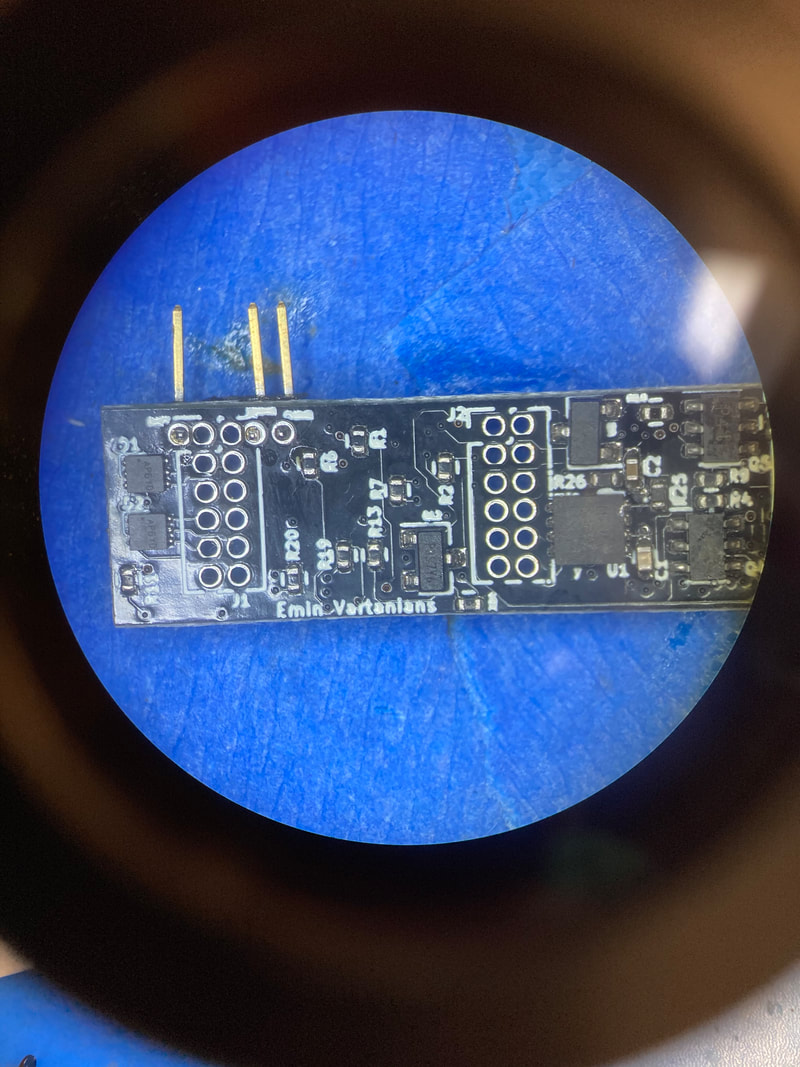
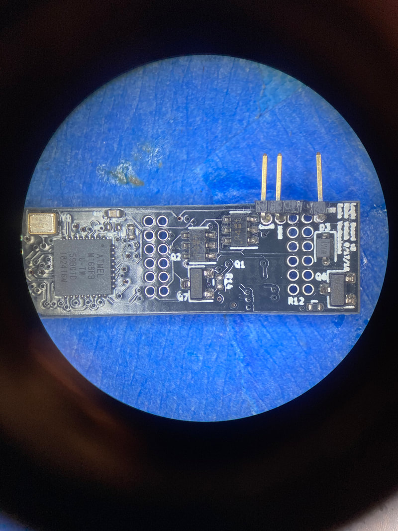
Had a hell of a time debugging a couple boards because they just wouldn't boot up or wouldn't talk back or wouldn't make their 180v. Did some digging and inspections and was shocked to find that a ton is wrong with the boards! First I noticed that the a resistor is not populated on the logic board, then the oscillator was flipped 180 deg, then a 1M ohm resistor was populated on a 10k spot, and finally I found a cracked capacitor! Pretty fed up with the Chinese boards I ordered. I sent a BOM and everything and it seems like the active components are correct but the passives could totally be cheapo counterfeits or not correctly rated (hence the cracked via) or bad tolerances. As I probed I found a 100nF part instead of a 10nF part on the charge pump. I took a few 10nF parts that were working correctly at the charge pump and tested them for about 70 hours straight with 180v on them. The 10nF caps in the charge pump are supposed to be 200v rated so the one that cracked might have been rated for a lower voltage. I suspect they bought the right parts but just populated them in the wrong spots. So now I gotta probe every terminal and make sure. I also realized that Q10 is missing! like I completely deleted the pads for it and the traces just stop at a certain place, so gonna have to manually place those. Don't know what happened, pretty rookie mistake but I guess no one is design reviewing my work...would have wanted the board house to catch that though, then again they loaded parts on the wrong pads so can't really trust them. Will have to make some documentation for myself to keep it all straight, this is what production looks like!
Had a hell of a time debugging a couple boards because they just wouldn't boot up or wouldn't talk back or wouldn't make their 180v. Did some digging and inspections and was shocked to find that a ton is wrong with the boards! First I noticed that the a resistor is not populated on the logic board, then the oscillator was flipped 180 deg, then a 1M ohm resistor was populated on a 10k spot, and finally I found a cracked capacitor! Pretty fed up with the Chinese boards I ordered. I sent a BOM and everything and it seems like the active components are correct but the passives could totally be cheapo counterfeits or not correctly rated (hence the cracked via) or bad tolerances. As I probed I found a 100nF part instead of a 10nF part on the charge pump. I took a few 10nF parts that were working correctly at the charge pump and tested them for about 70 hours straight with 180v on them. The 10nF caps in the charge pump are supposed to be 200v rated so the one that cracked might have been rated for a lower voltage. I suspect they bought the right parts but just populated them in the wrong spots. So now I gotta probe every terminal and make sure. I also realized that Q10 is missing! like I completely deleted the pads for it and the traces just stop at a certain place, so gonna have to manually place those. Don't know what happened, pretty rookie mistake but I guess no one is design reviewing my work...would have wanted the board house to catch that though, then again they loaded parts on the wrong pads so can't really trust them. Will have to make some documentation for myself to keep it all straight, this is what production looks like!
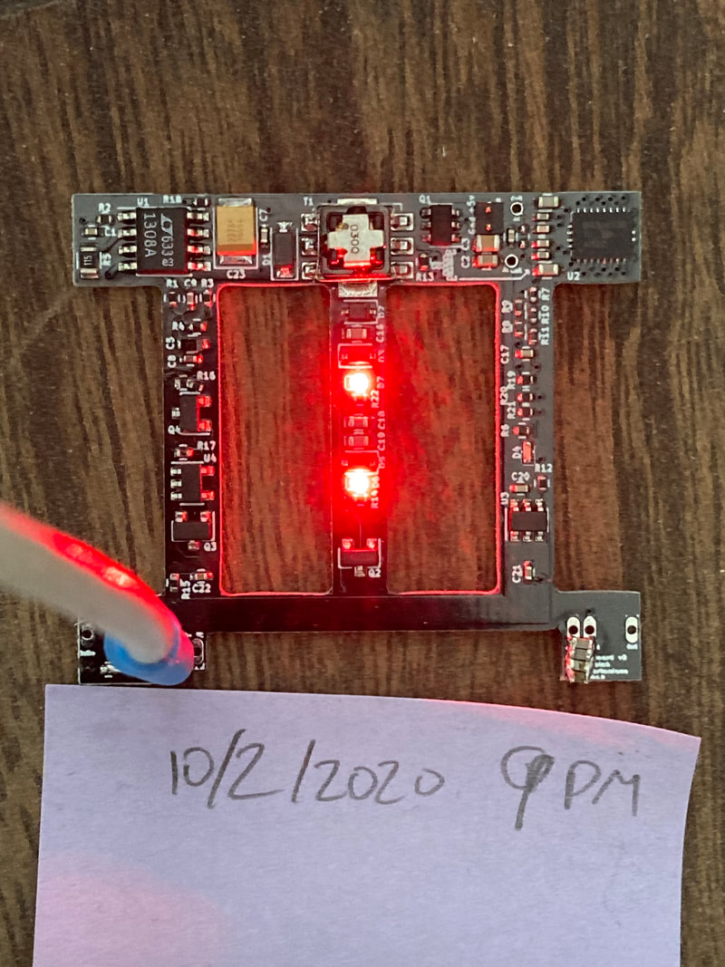
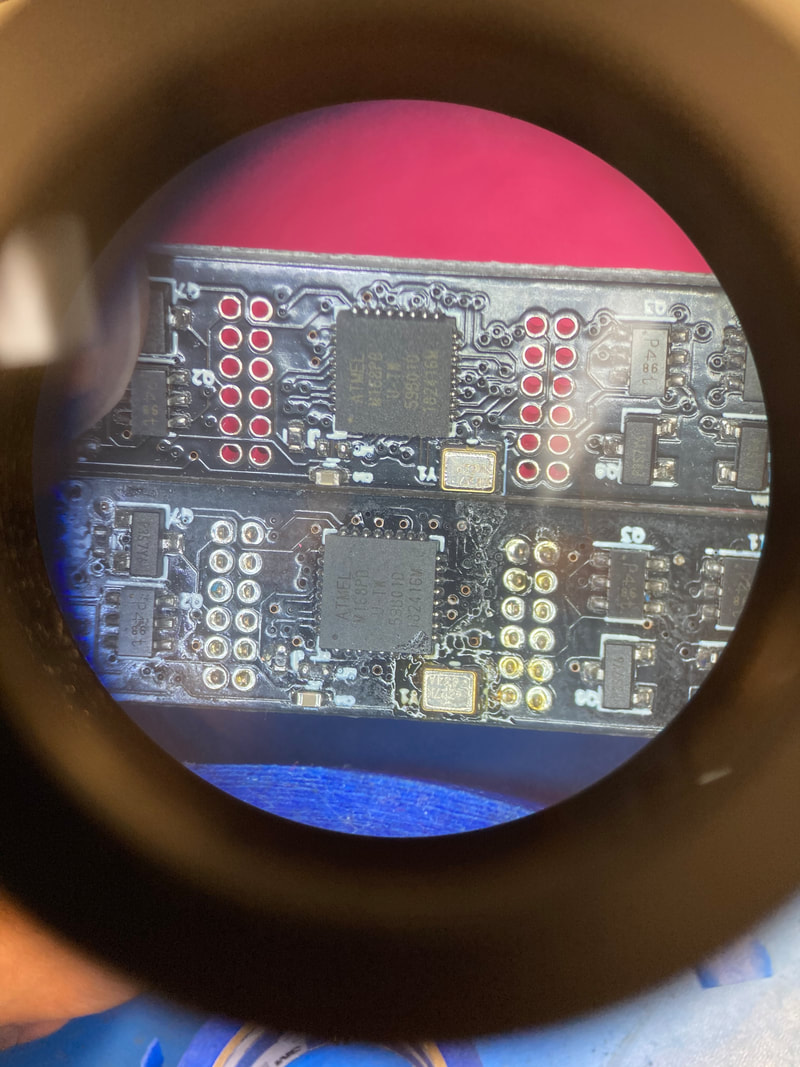
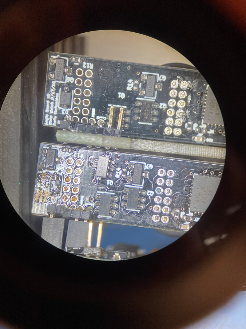
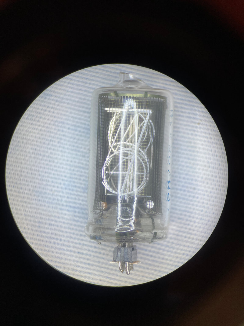
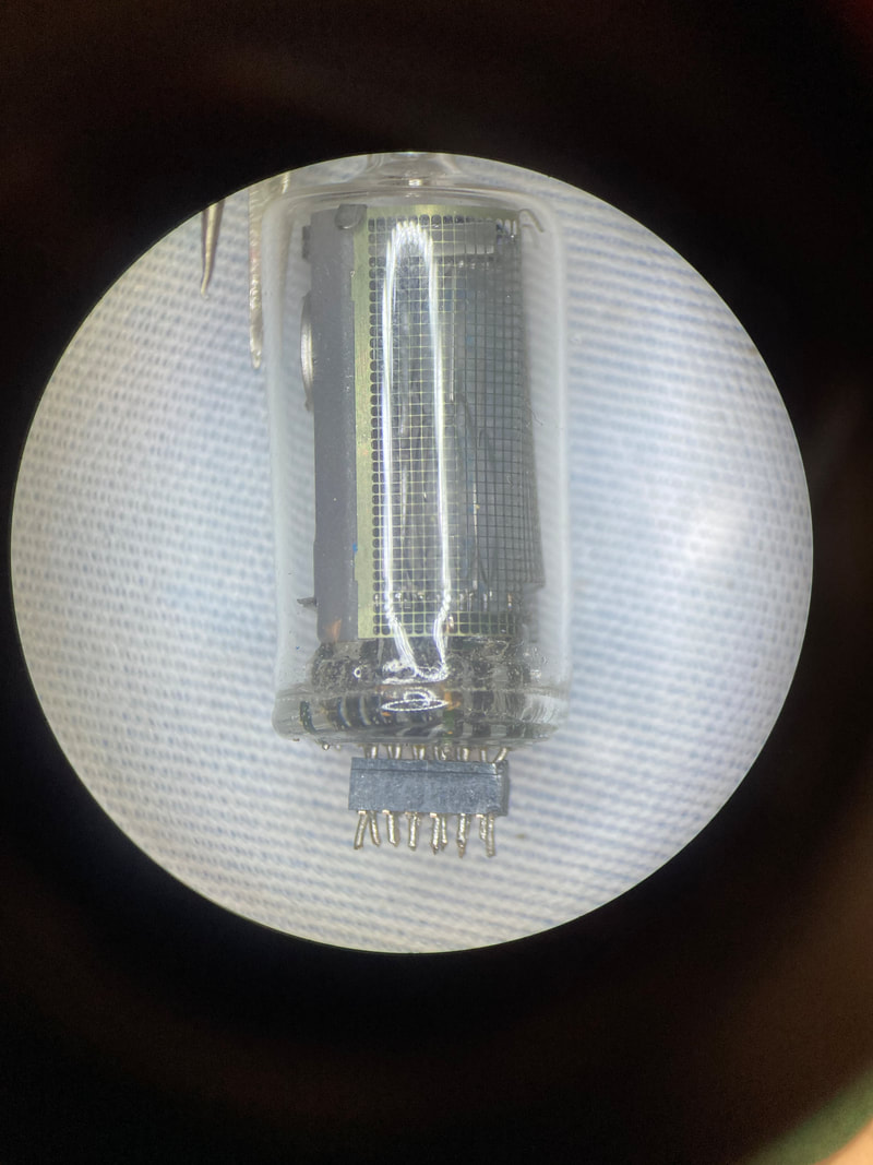
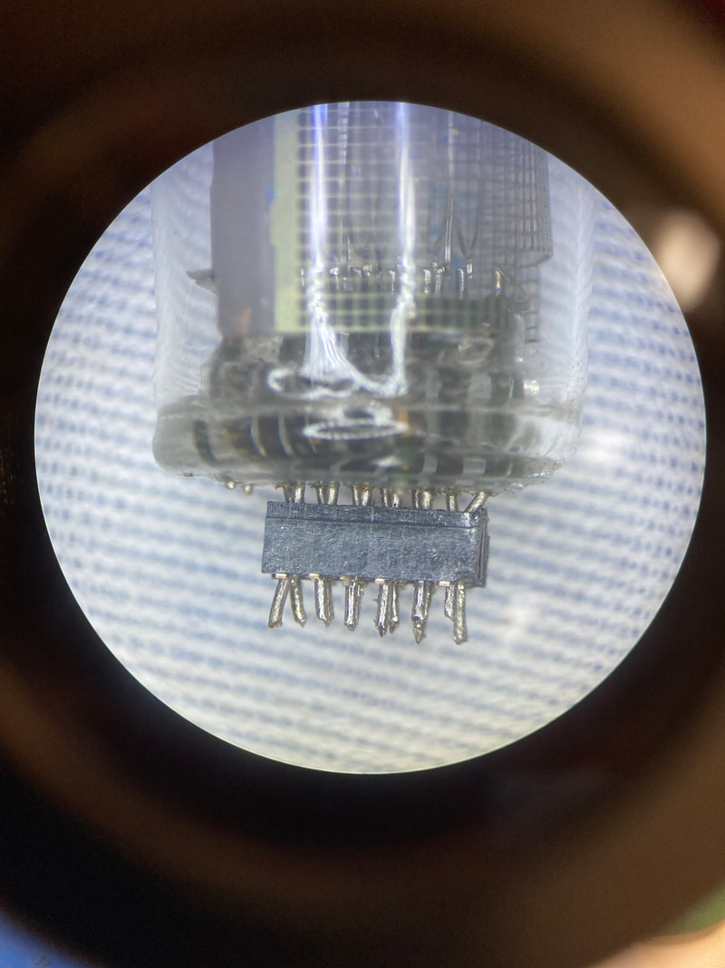
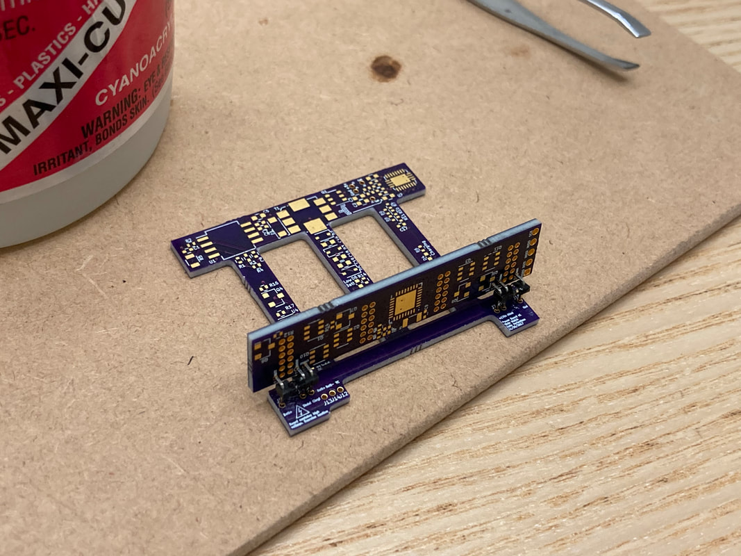
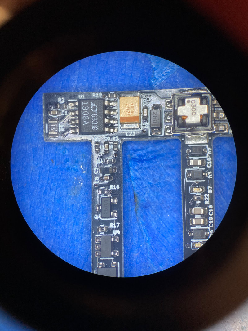
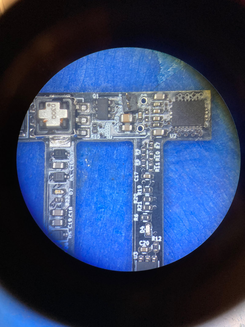
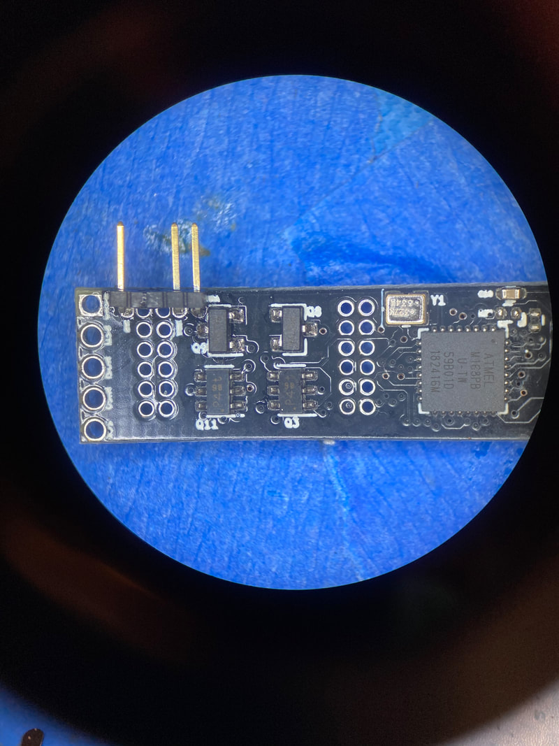
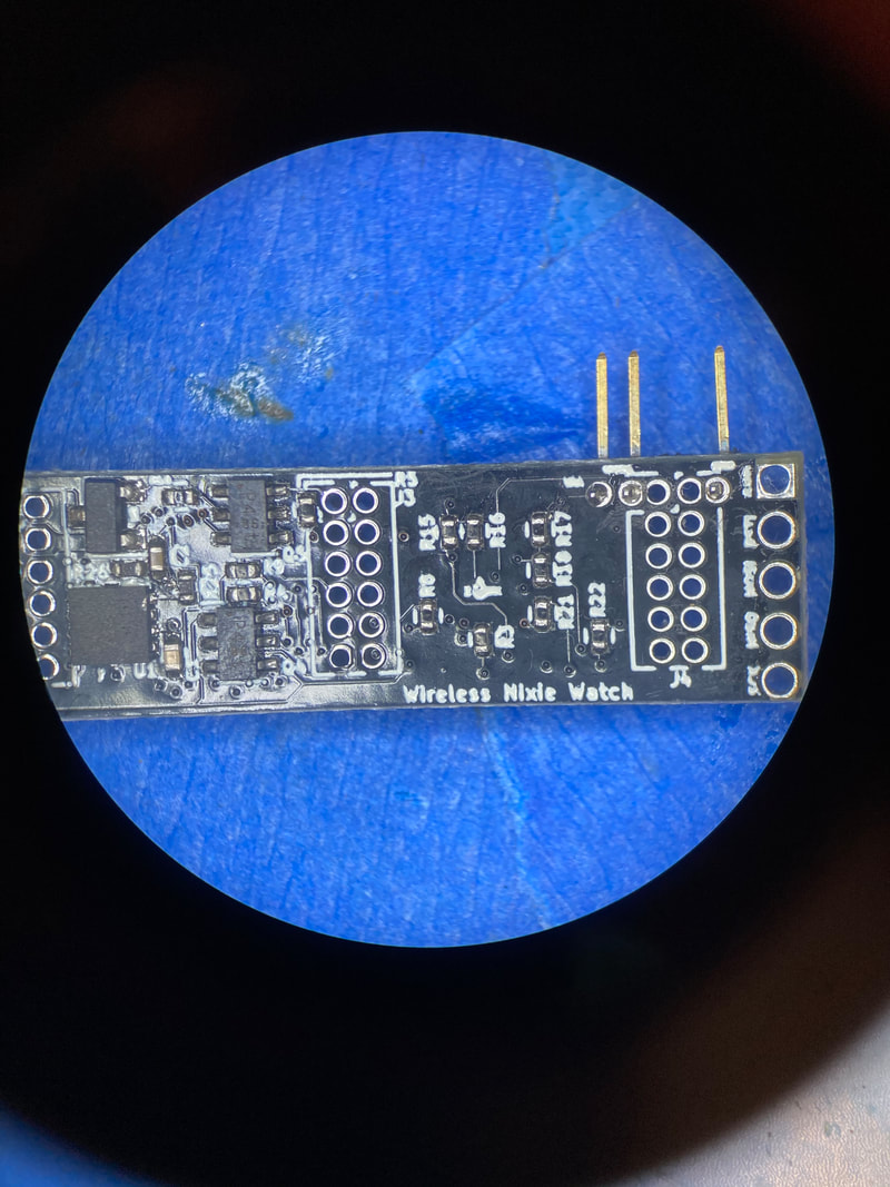
Realized I never gave you a peek at the production boards so here's a parade.
| | |
Battery
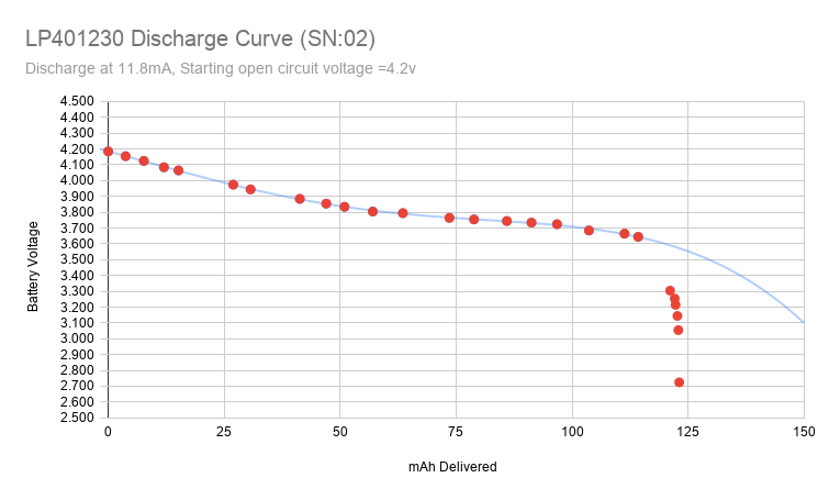
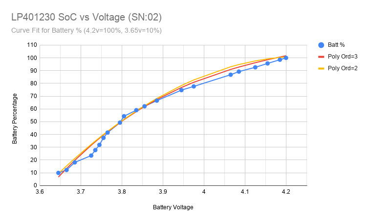
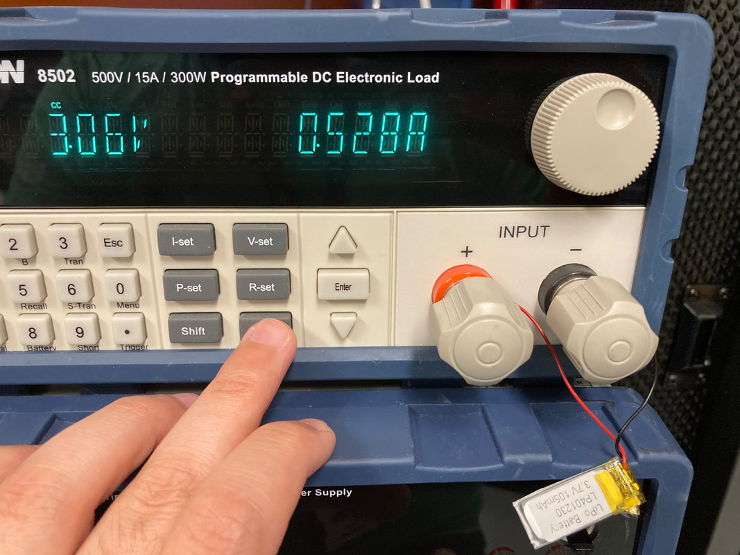
I did some real battery work and measured the discharge curve of the cells. You put a constant current discharge over the cell from full to dead and see the voltage drop, then map the discharge in mA to how much time has passed and achieve the correct mAh rating and SoC curves. I pulled 11.8mA for almost 10 hours (you want to be around 1/10 C so you don't stress the chemistry or tabs). There's definitely a sharp knee around 3.65v so I'll mark that as the 10% mark where I don't fire the tubes anymore. Then I marked 4.2v as 100%, scaled capacity to percentages and fit a curve to whole thing excluding below my 10% mark.
I did some real battery work and measured the discharge curve of the cells. You put a constant current discharge over the cell from full to dead and see the voltage drop, then map the discharge in mA to how much time has passed and achieve the correct mAh rating and SoC curves. I pulled 11.8mA for almost 10 hours (you want to be around 1/10 C so you don't stress the chemistry or tabs). There's definitely a sharp knee around 3.65v so I'll mark that as the 10% mark where I don't fire the tubes anymore. Then I marked 4.2v as 100%, scaled capacity to percentages and fit a curve to whole thing excluding below my 10% mark.
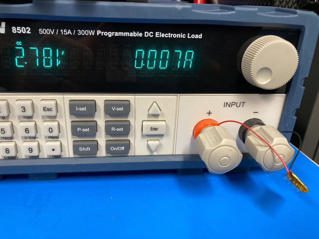
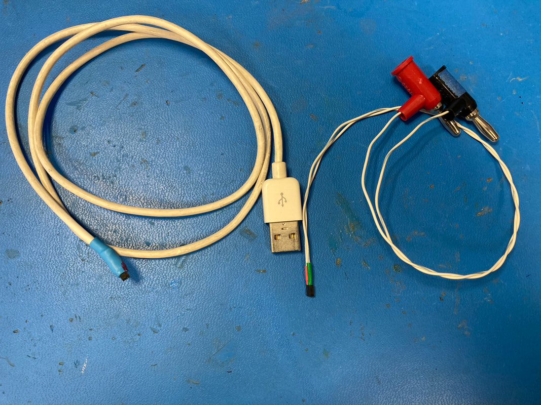
I also tried to characterize the battery protection module (PCM?) that I'm choosing not to take off. Seems like it's robust and not too restrictive. I pulled half an amp through it for a couple seconds and watched the cells go down to 2.78v before cutting out. The protection circuit then needs to be charged to let the battery source current again. You can also see the connectorized headers I made for the battery and 5v input through a USB. Always needs test cables!
Battery Sense Line
I wanted to test out the new battery sensing with the mosfet controlled voltage divider. Once I fixed all the parts there were incorrectly populated I got a cool view of how long things take on the microcontroller to get ADC readings. I currently turn on the mosfet then read the 3 accel axes before reading the batt sense line. I figured this would give the tiny 97uA time to settle out but the impedance is low enough to settle the voltage within like 2us. I also notice a weird tick up at the end when I turn off the mosfet...not sure why, there are no inductive elements here. You can see the whole things takes about 620us which doesn't fit into my understanding of the 1Mhz system clock being divided down to 125khz ADC clock and how many cycles it takes to read the 4 channels I'm reading. I'll have to investigate this more next time. You can also see a tiny blip down around 500us where the voltage droops for a very short period of time. 125khz translates to 8us which kindaaaa looks to be the length of the droop. anyway, will investigate a bit more next time. I also noticed that the 3.3 LDO I'm using varies its exact voltage board to board so I might have to deploy custom code to read the ADC for each board. Thought about using the internal 1.1v ref in the microcontroller as my Aref but then I'd have to voltage divide all over the place to get signals down to that range, not worth it.
I wanted to test out the new battery sensing with the mosfet controlled voltage divider. Once I fixed all the parts there were incorrectly populated I got a cool view of how long things take on the microcontroller to get ADC readings. I currently turn on the mosfet then read the 3 accel axes before reading the batt sense line. I figured this would give the tiny 97uA time to settle out but the impedance is low enough to settle the voltage within like 2us. I also notice a weird tick up at the end when I turn off the mosfet...not sure why, there are no inductive elements here. You can see the whole things takes about 620us which doesn't fit into my understanding of the 1Mhz system clock being divided down to 125khz ADC clock and how many cycles it takes to read the 4 channels I'm reading. I'll have to investigate this more next time. You can also see a tiny blip down around 500us where the voltage droops for a very short period of time. 125khz translates to 8us which kindaaaa looks to be the length of the droop. anyway, will investigate a bit more next time. I also noticed that the 3.3 LDO I'm using varies its exact voltage board to board so I might have to deploy custom code to read the ADC for each board. Thought about using the internal 1.1v ref in the microcontroller as my Aref but then I'd have to voltage divide all over the place to get signals down to that range, not worth it.
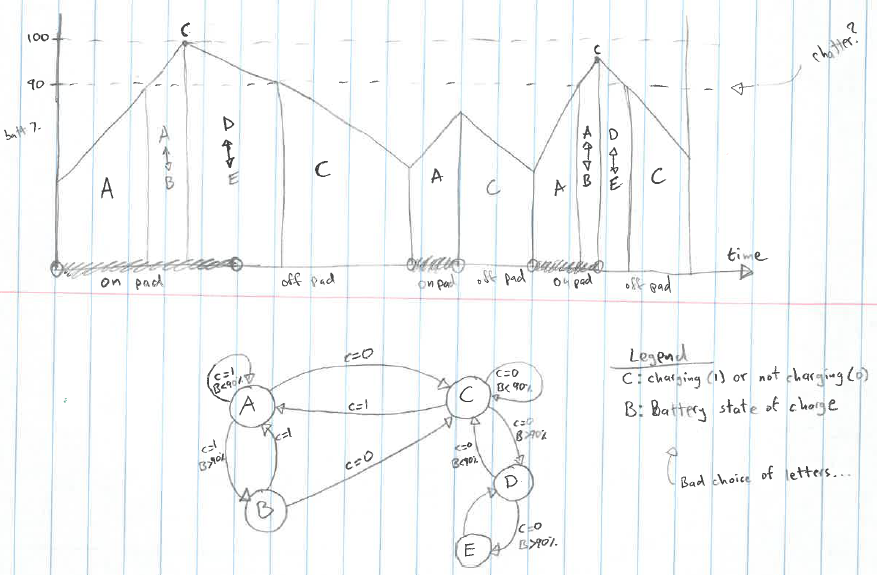
Charge States and State Diagrams
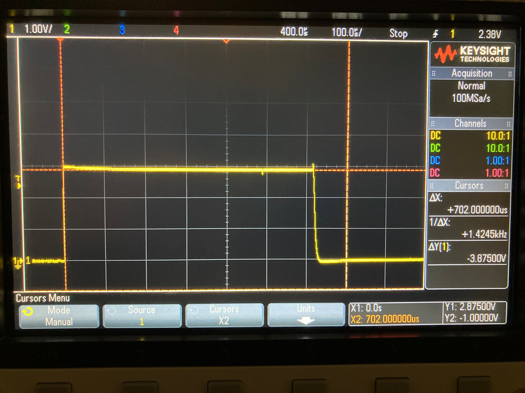
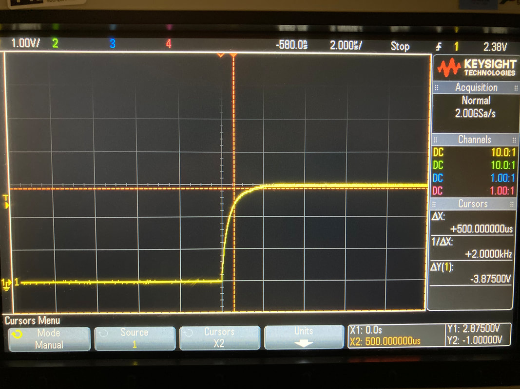
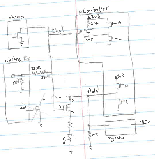
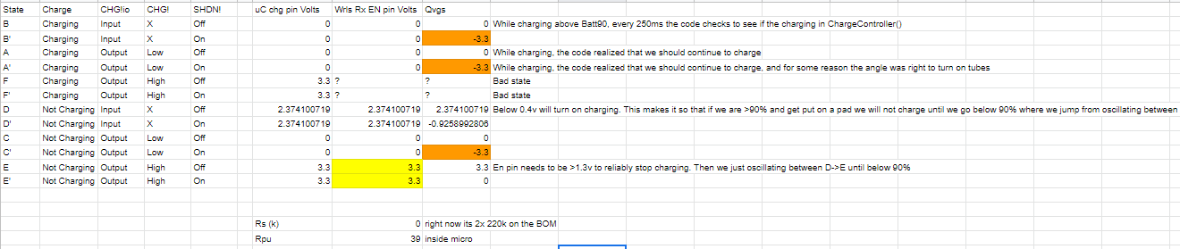
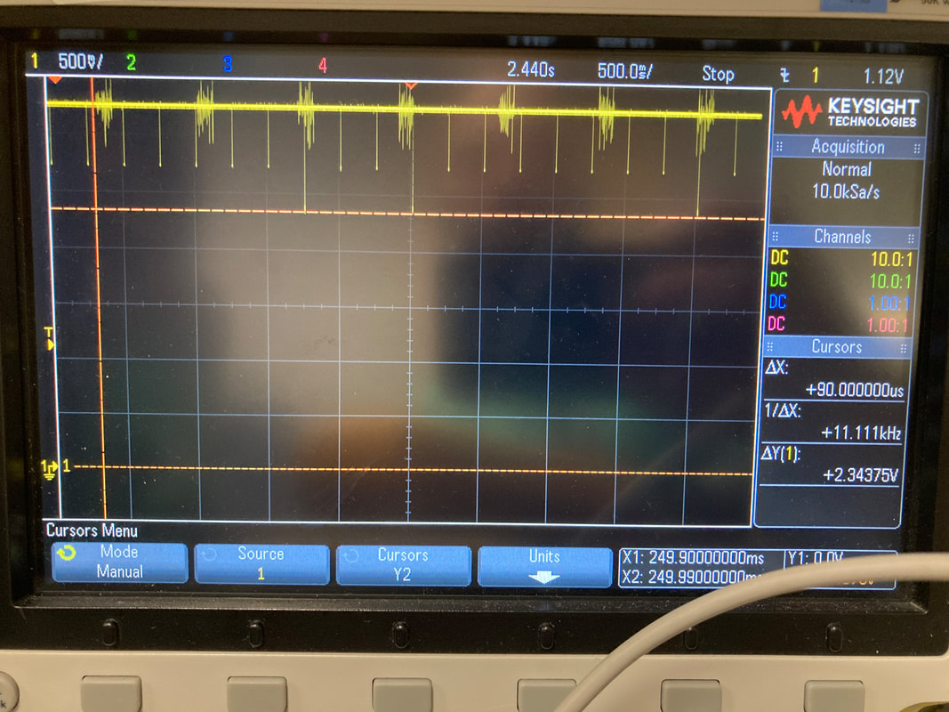
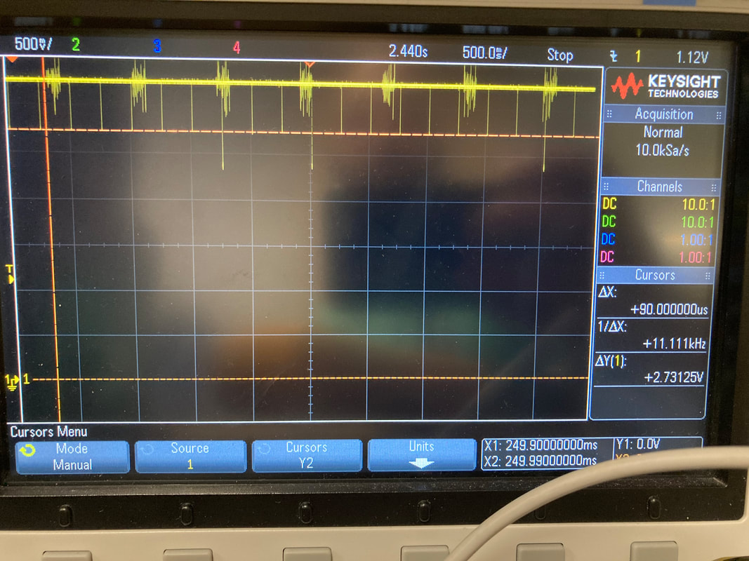
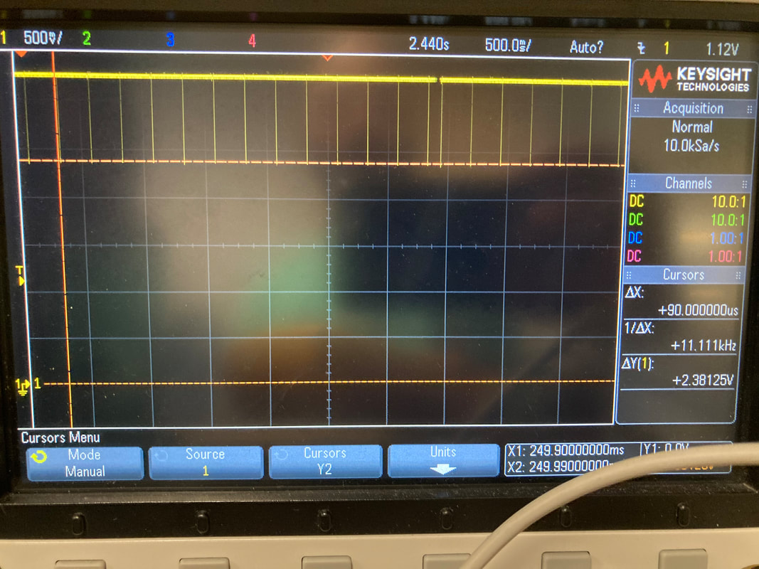
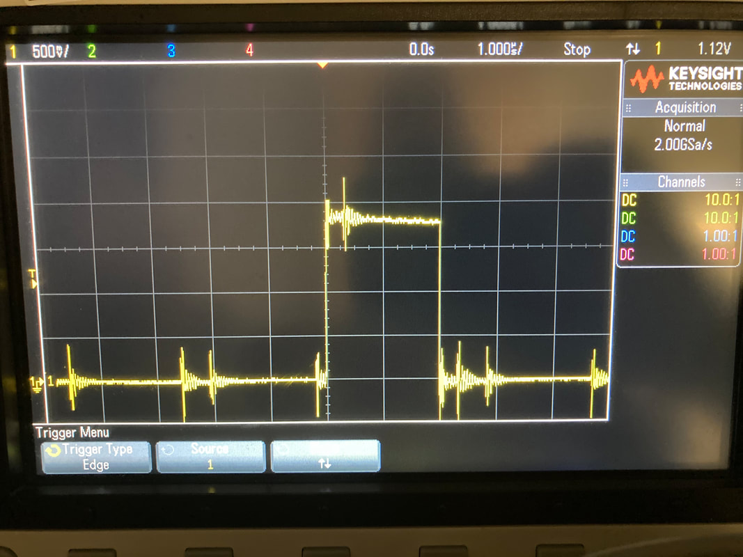
Man I hope to do this less cleverly next time around. Figuring out when I'm charging and when to tell the Tx coil to stop sending power all on the same line has been too clever for its own good. I'm using the fact that the lipo charging chip has an open drain pulldown to indicate if its charging to sense whether or not my charge is complete or if I need to charge. The whole thing revolves around this batt90, 90% SoC. If I'm below that line then I don't care about the charging chip, just give me power. If I'm above that line then every time I run the ChargeController() routine I'm going to set the CHG! line as an input and have an internal pull up on it so I can sense if the lipo charger is pulling it down (charging) or the pin is floating and subject to my voltage divider (not charging). If I can discern between those states without messing up the EN1/2 pins on the wireless Rx chip then I have succeeded in using this one line of copper for two purposes and way to go me. There's a third use for this line actually, as the gate of the mosfet that controls the colon LEDs, but trying to have a state diagram for that scenario was going to be too complicated. If the colon LEDs are off while the tubes are on then the charging is going to be interrupted. This is just a limitation of the current design, I'll do it less cleverly next time. I got pictures of this in action for the case where we are not charging. You can see every 250ms in the scope shots that the 3.3v CHG! line dips down to something inn the 2v range as it reconfigures as an input and engages the ~50k pullup. I got two different voltages while the wireless charging was on, not sure why. But when I charged through the 5v USB I got a clean signal at 2.3v. This will help me figure out the actual value of that pullup in the mico and how I can tune the two 220k resistors I had originally put there.
Man I hope to do this less cleverly next time around. Figuring out when I'm charging and when to tell the Tx coil to stop sending power all on the same line has been too clever for its own good. I'm using the fact that the lipo charging chip has an open drain pulldown to indicate if its charging to sense whether or not my charge is complete or if I need to charge. The whole thing revolves around this batt90, 90% SoC. If I'm below that line then I don't care about the charging chip, just give me power. If I'm above that line then every time I run the ChargeController() routine I'm going to set the CHG! line as an input and have an internal pull up on it so I can sense if the lipo charger is pulling it down (charging) or the pin is floating and subject to my voltage divider (not charging). If I can discern between those states without messing up the EN1/2 pins on the wireless Rx chip then I have succeeded in using this one line of copper for two purposes and way to go me. There's a third use for this line actually, as the gate of the mosfet that controls the colon LEDs, but trying to have a state diagram for that scenario was going to be too complicated. If the colon LEDs are off while the tubes are on then the charging is going to be interrupted. This is just a limitation of the current design, I'll do it less cleverly next time. I got pictures of this in action for the case where we are not charging. You can see every 250ms in the scope shots that the 3.3v CHG! line dips down to something inn the 2v range as it reconfigures as an input and engages the ~50k pullup. I got two different voltages while the wireless charging was on, not sure why. But when I charged through the 5v USB I got a clean signal at 2.3v. This will help me figure out the actual value of that pullup in the mico and how I can tune the two 220k resistors I had originally put there.
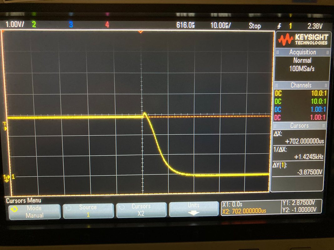
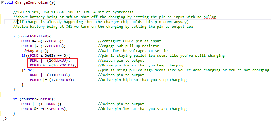
I thought this was super cool to see in action. My ChargeController() code is show below, you can read the comments to see what it does and why it does it. I kept getting very short bursts of pullup on the scope while charging above 90% SoC which was surprising to me. When I zoomed in I saw they the burst was for 2us exactly...coincidence that it's two system clock ticks (1Mhz), I think not! After staring that the code for 10 seconds it was obvious and a really cool view into the way register values latch and execute in microcontrollers. The part of the code I've boxed is the problem. a couple lines above I set the data direction register for that pin as an input then I write a 1 into the PORTD3 spot on PORTD register which engages the 50k pullup. Then, if I see that the pin is staying low I know to drive the pin low myself right? well I set the data direction register as an output so I can drive it low. The pin value (1 or 0) if the port is set as an output is controlled by PORTD register, same register as engaging the 50k pullup or not when the pin is an input. So you can clearly see on the scope plot that it takes 2 clock cycles between the pin changing input->output and the PORTD3 value in the register to go from 1->0. This was fascinating to me and just another example of why I love working with microcontrollers and bare metal C. You get to be right there in the registers, complete control (and complete culpability!). Easy peasy solution is to reverse the lines in the box so I de-assert the pullup before I drive the pin low.
Next Steps
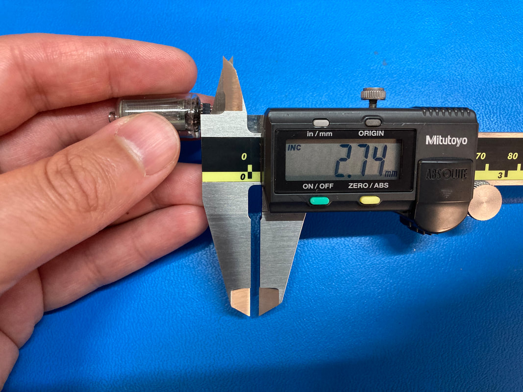
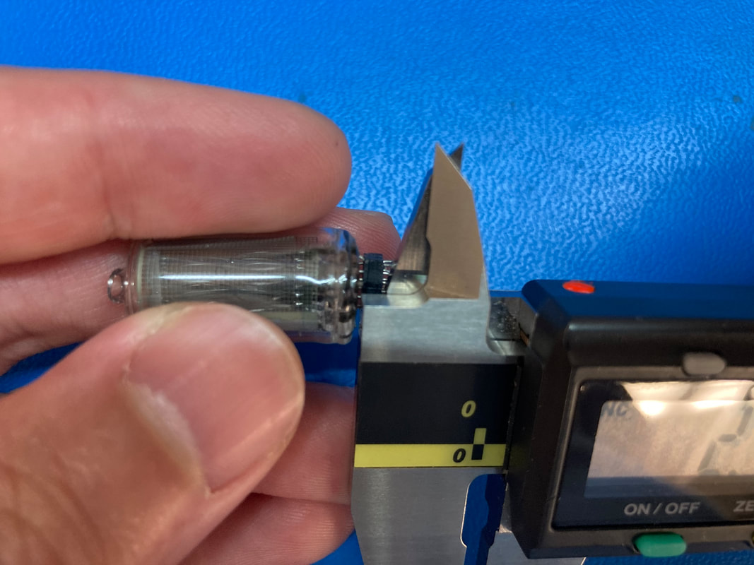
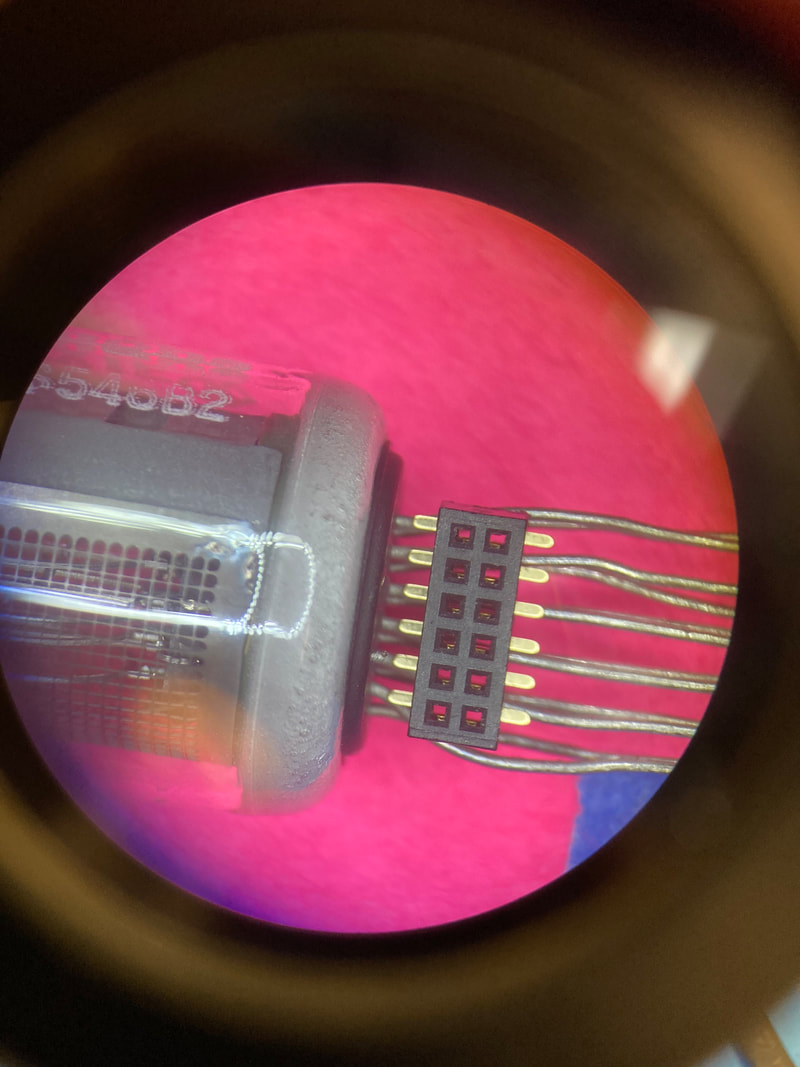
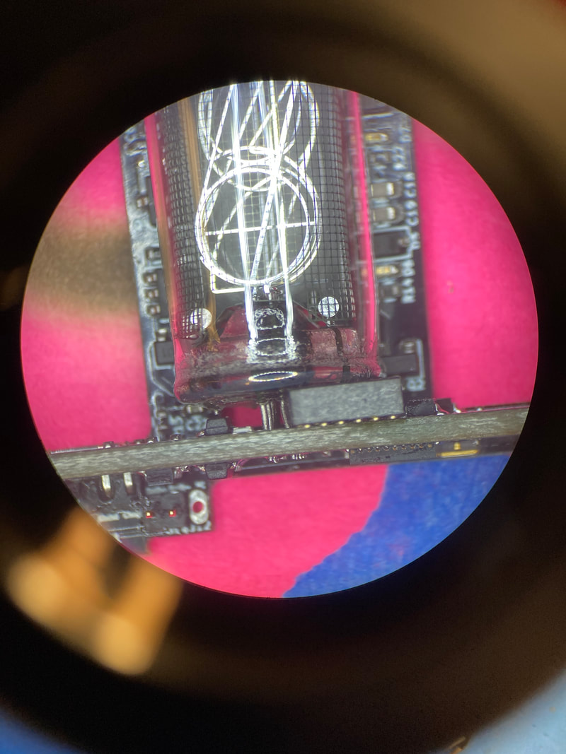
I got a lot cooking up already. Realized I should serialize the boards so I can reference them easier (should have known that from being a big boy engineers...dummy). I'm doing a ton of testing on glues and water tightness for holding the glass to the case so I think next post will be a lot of that. I'm thinking about the next revision of the watch (if it takes off... we'll see) should have connectorized nixie tubes so looking into short profile headers. Found a really good one with 1mm pitch which is perfect match for these tubes but the male header pin that's supposed to mate to these has a size of 12mils whereas the tube leads are 16 mils so I'm having a really hard time with the test fit. I'm also slowly building up the first production unit which is exciting, finding out how to best make these consistently... wish I knew a manufacturing engineer haha. I made a bunch of right angle connectors and noted that if I have another go at this design I'd make the connector spacing match a wider connector such that I'd have to just unpopulate contacts, instead of cutting and gluing two pieces together to get the length right. Lastly, I keep finding that my SN00 unit's right angle connections keep failing which is sad. This is caused by the original watch having had a really bad cant between logic and power board such that the case actually adjusted them closer to 90 deg and the cover glass and tubes were taking up the mechanical load... not good. So now I'm seeing that it won't charge because for some reason some trace that controls the charging (gnd, batt+, CHG!, etc) is severed on the board so it won't be charging then I'll push on the tubes or something and it'll start because the trace that's cut just made a connection again. Will try to fix it since it's SN00 and its sentimental but the production units shouldn't have this problem. Ok this turned into a really long post. See you guys next time!
I got a lot cooking up already. Realized I should serialize the boards so I can reference them easier (should have known that from being a big boy engineers...dummy). I'm doing a ton of testing on glues and water tightness for holding the glass to the case so I think next post will be a lot of that. I'm thinking about the next revision of the watch (if it takes off... we'll see) should have connectorized nixie tubes so looking into short profile headers. Found a really good one with 1mm pitch which is perfect match for these tubes but the male header pin that's supposed to mate to these has a size of 12mils whereas the tube leads are 16 mils so I'm having a really hard time with the test fit. I'm also slowly building up the first production unit which is exciting, finding out how to best make these consistently... wish I knew a manufacturing engineer haha. I made a bunch of right angle connectors and noted that if I have another go at this design I'd make the connector spacing match a wider connector such that I'd have to just unpopulate contacts, instead of cutting and gluing two pieces together to get the length right. Lastly, I keep finding that my SN00 unit's right angle connections keep failing which is sad. This is caused by the original watch having had a really bad cant between logic and power board such that the case actually adjusted them closer to 90 deg and the cover glass and tubes were taking up the mechanical load... not good. So now I'm seeing that it won't charge because for some reason some trace that controls the charging (gnd, batt+, CHG!, etc) is severed on the board so it won't be charging then I'll push on the tubes or something and it'll start because the trace that's cut just made a connection again. Will try to fix it since it's SN00 and its sentimental but the production units shouldn't have this problem. Ok this turned into a really long post. See you guys next time!